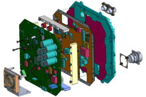
FREEDOMCAD will be exhibiting at PCB West 2025, Booth 308, October 1st, Santa Clara Convention Center
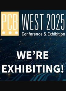
Visit us in Booth 308 on Wednesday, October 1st, 2025. We are excited to announce that we will be attending PCB West on October 1st at the Santa Clara Convention Center, visit us at Booth 308. Join us to explore the latest advancements in PCB technology, attend educational sessions, and connect with industry leaders. We look… Read More »